Intel 4 process node detailed, double density with 20% higher performance
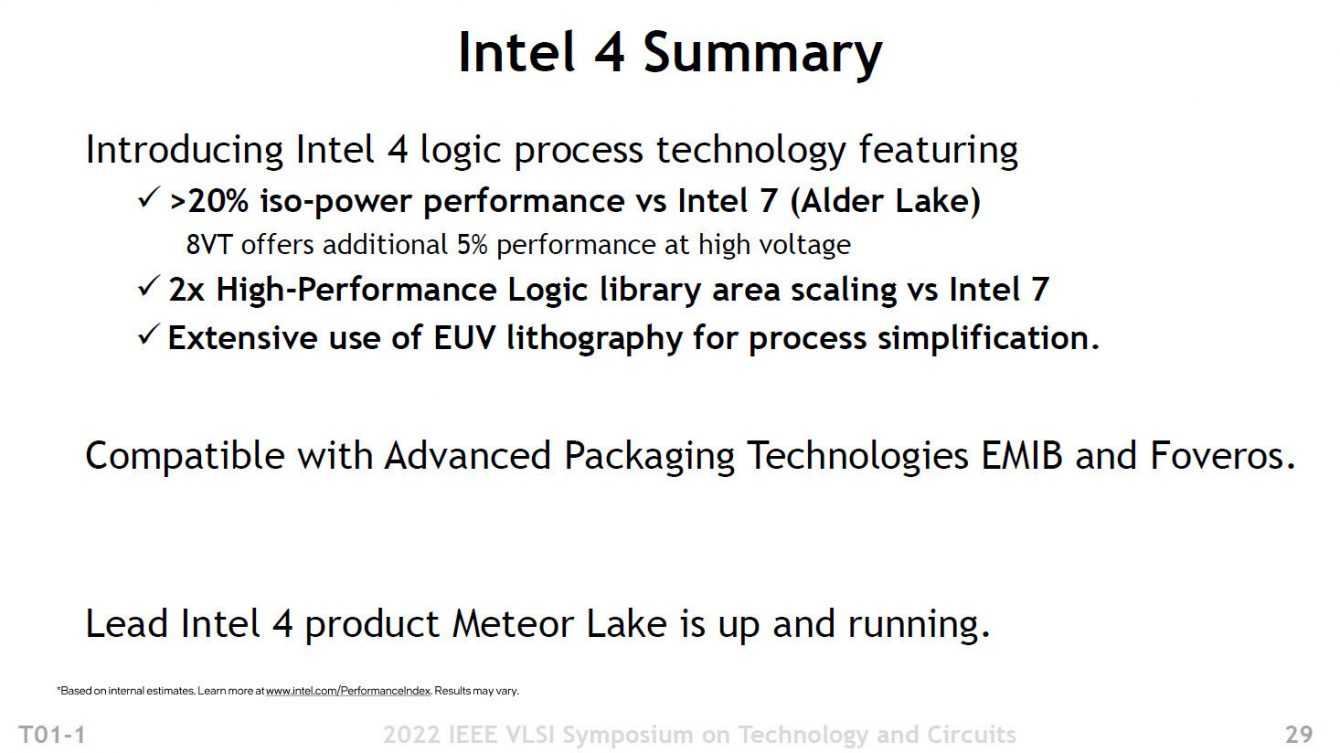
I Intel semiconductor nodes (here for more information on the company) were quite controversial with the arrival of the design a 10 nm. After years of work, the knot has been delayed several times and, only recently, the general public has gotten the first ones chip since 10 nm. Today, at the annual symposium VLSI dell’IEEEwe get more details on the next ones Intel nodes, called Intel 4. Previously referred to as a 7nm process, Intel 4 is the company’s first node to use the EUV lithograph accompanied by various technologies. The first thing when a new process node is discussed is the density. Compared to Intel 7, Intel 4 will double the number of transistors for the same area and will allow transistors with 20% higher performance.

Technical details of the new Intel process node 4
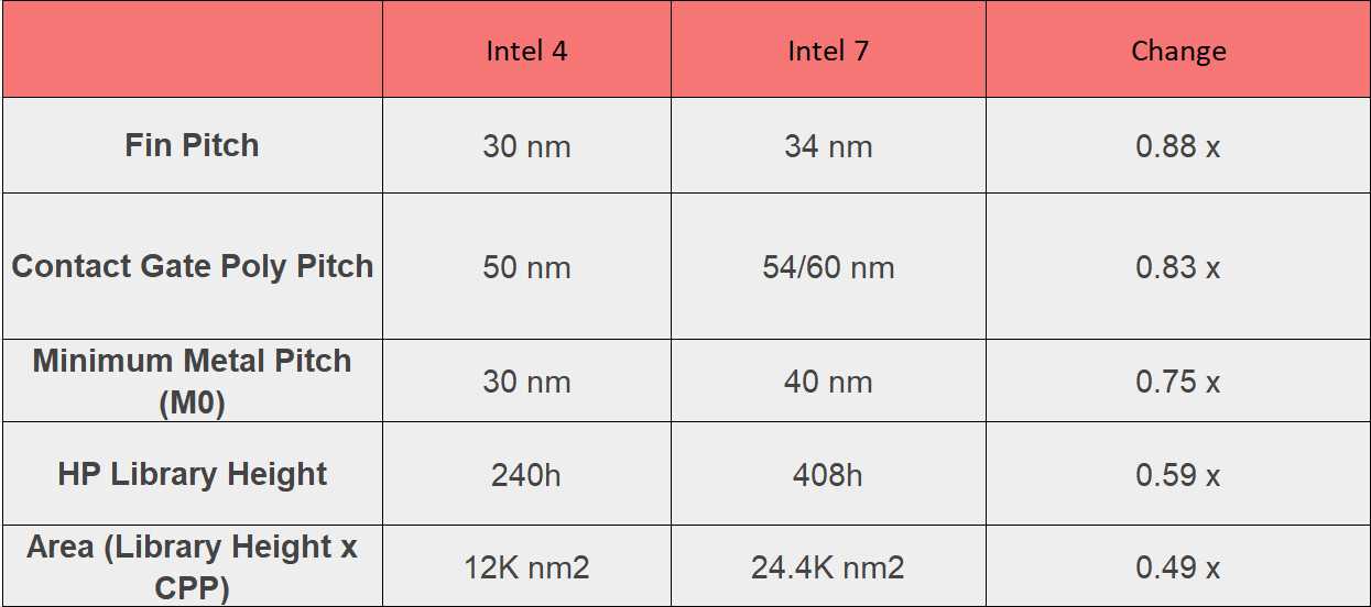
Considering the size of the individual transistors, the new Intel Node 4 represents a tiny piece of silicon that is even smaller than its predecessor. It is composed of a fin pitch of 30 nma step Poly Contact Gate di 50 nm between the gates and a minimum metal pitch (M0) of 50 nm. These make the Intel 4 transistor significantly smaller than Intel cell 7. For scaling, Intel 4 provides twice the number of transistors in the same area as Intel 7. However, this reasoning only applies to logic.
For the SRAM, the new PDK provides an area reduction of 0.77, which means that the Intel 7-based SoC itself will not be half the size of Intel 4. This is because SRAM plays a significant role in chip design. The Intel 7 HP library can put 80 million transistors on a square millimeter, while the Intel 4 HP is capable of 160 million transistors per square millimeter.
Transistor e EUV
As for the individual transistor levels, Intel has been having fun with them as the company has now put in 16 layers of metal for logic in Intel node 4, compared to 15 in Intel 7 PDK. The gate is made of tungsten, while the top four metal layers are made of copper with cobalt coating. This guarantees better performance than plain copper. For the remaining layers, for the interconnection of the wiring is used pure copper.
In the Intel 4 production process, the company uses for the first time EUV obtaining excellent results. The number of steps to produce the chip is now reduced and the number of jigs for engraving is said to be reduced by 20% compared to Intel 7, thanks to more powerful EUV lithography tools. Were it not for EUV, the number of masks for this type of transistor would have to increase by 30% since the process of multi-patterning is very complicated.

Performance and earnings
Last but not least, there are the performance of these new transistors. To a power iso of 0.65 VoltsIntel reports a gain of the 21,5% in sustainable frequency with Intel 4 than Intel 7. At higher power like 0,84 Volt, the curve flattens out with an improvement of about 10%. For iso frequency tests, the company reports a lower power consumption of the 40% measured at a transistor switching rate of 2.1 GHz.
The first products based on the new node will sometime arrive in 2023, with Meteor Lake-P projects hitting shelves first. Others are expected to follow SKU and we can’t wait to see how good this semiconductor manufacturing node will be.
And what do you think of this new one Intel process node 4 ? tell us yours below in the comments and stay connected on TechGameWorld.com, for the latest news from the world of technology (and more!).
Article Intel process node 4: in detail, the news from Intel comes from TechGameWorld.com.


Leave a Reply
View Comments