The wait for NVIDIA’s GeForce RTX 4080 graphics card is great, and as the presentation approaches, the rumors increase, now, on the PCB!
Up until now we had witnessed rumor’s inherent in performance, GPU and its structureand even on the hypothetical design of the future near-top range of the Nvidia list, this time we speak instead of PCB, which is very important in order to analyze its structure.
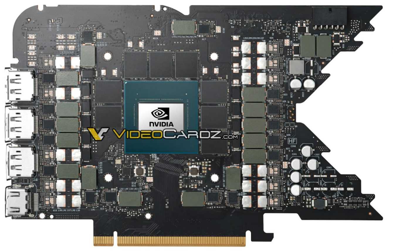
He shoots an image online, then made known more by the videocardz portal, by a PCB where an AD103 GPU Chip is mounted on itwhich should be right from the GeForce RTX 4080.
The PCB of the future GeForce RTX 4080 (Founders Edition of course) has many components, but several elements appear missing. Example, if we observe the phases, since they should be 27 theoretically, only 17 appear, easily observable from the empty soldering points. This inevitably leads to the hypothesis that the PCB, and in more detail the Chip AD103 and its structure, have the potential to support even greater powers, and any higher technical specifications, the speculation is that the AD103 Chip can also adapt to a possible RTX 4080 Ti model. Even the capacitors, if we observe, are present only in reduced quantity compared to the potential possibility offered by the PCB.
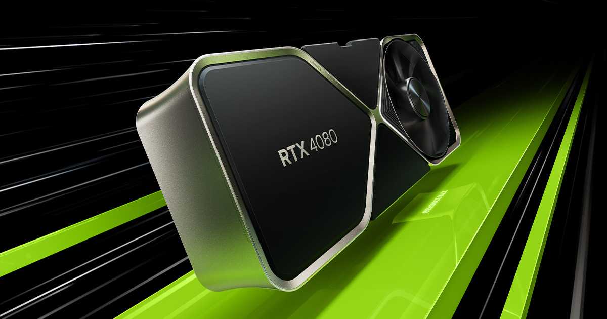
NVIDIA GeForce RTX 4080: the PCB appears on the net!
The asymmetrical shape of the PCB is identical to that of the RTX 4090, which has been rumored for some timehave the same dimensions and the same layout of the mounting holes of the heatsink. This means that a possible third party partner can use this PCB as a primary sample, and it will be much easier to adapt a design for an eventual cooler. However, we haven’t seen any RTX 4090s with a ‘V’ shaped PCB yet and they are all rumors.
Analyzing the PCB, we note that it presents 8 GDDR6X memory modules positioned around the AD103 GPU. This is the area that has been most modified compared to the PCB of the RTX 4090 FE. The RTX 4080 has a memory bus a 256 bit we remember, and for that each of the modules contains 2 GB of capacity for a total of 16 GB of VRAM. It is worth mentioning that this card has an unusual memory clock speed of 22,4 Gbps, not 23 Gbps canons.

The card then has a 12VHPWR 16-pin power connector located at the same point as the RTX 4090, just look at the top right. It is important to note that almost all RTX 4080 cards for sale will ship with a 3 × 8 pin to 16 pin adapter, and not 4 × 8 pin like the RTX 4090. This model has a Default TDP of 320W, but some custom models may go up to 380W. The RTX 4080 is equipped with 9728 CUDA coreswhich represent a 5% reduction in the number of cores compared to the full AD103 GPU. We will see during the official presentation if all this is confirmed.
If you want to continue to know the latest news from the hardware world, keep following us. Greetings from TechGameWorld.com.
The article NVIDIA GeForce RTX 4080: the PCB appears on the net! comes from allotek.




Leave a Reply
View Comments