
A recently registered patent could confirm that the new AMD RDNA 3 GPUs could take advantage of a chiplet design based on a technology called AMD Active Bridge
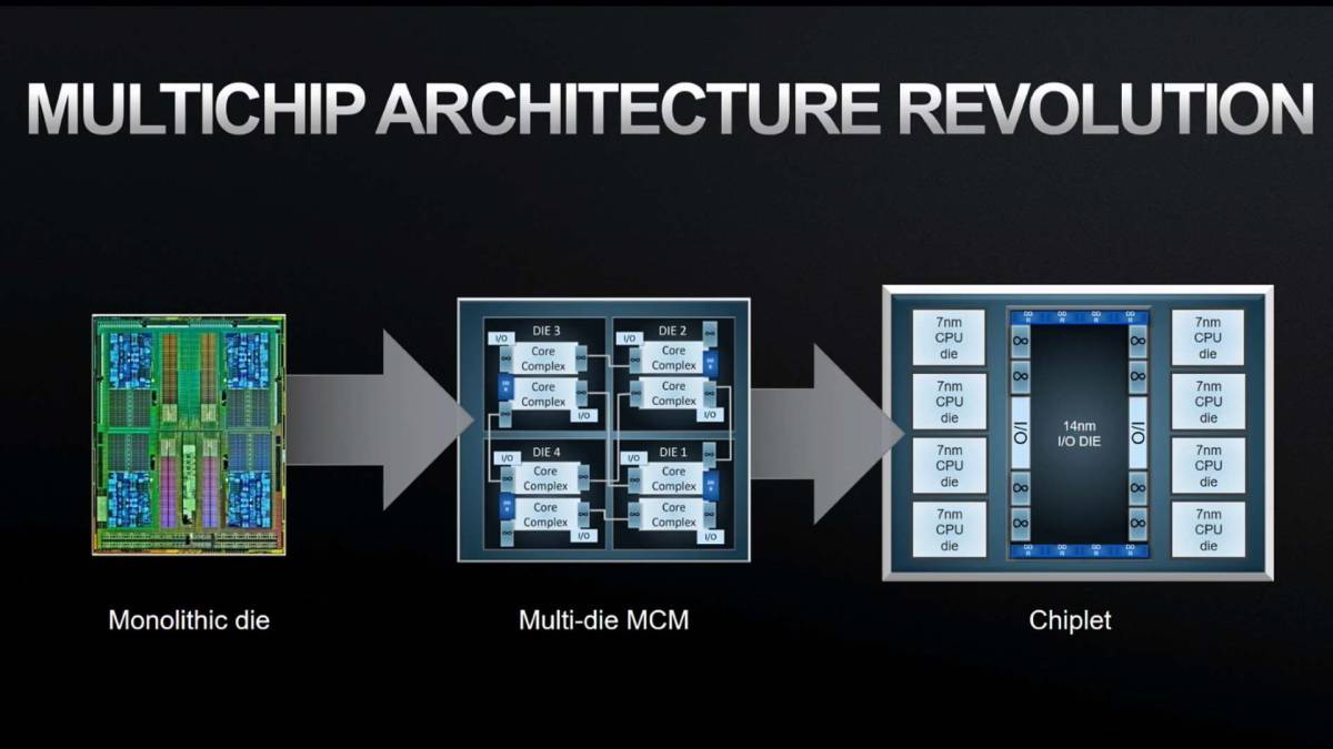
Initially the development of semiconductors was based on the possibility of integration an increasing number of transistors and components within the same chip, the principle on which Moore’s law is also based. Today, however, as we get closer and closer to infinitesimal component sizes, this trend is destined to slow down, but to compensate for it a different strategy is being considered. That of chiplets. It is essentially about produce the chips with a modular approach and then combine them together in the same package via a high performance communication interface to create the final product. AMD already uses this strategy for its high-end CPUs with a high number of cores, but soon the idea should also migrate to chiplet GPUs with the AMD RDNA 3 architecture. be ahead with development.
AMD RDNA 3: the new GPUs with AMD Active Bridge Chiplet?
The colleagues at wccftech let us know that AMD has issued a new patent concerning an active chiplet that acts as a bridge between multiple GPU dies, likely a technology that will underpin the AMD RDNA 3 architecture. AMD claims it has to tackle a problem similar to running multiple GPUs in parallel efficiently and the thing is not at all easy if we think of Crossfire which was a redundant technology like other multi-GPU implementations then abandoned. To solve this problem and to make it easy to implement a chiplet design of the new RDNA 3 GPUs, AMD proposed an active bridge that would connect multiple GPU chiplets together.
The main block diagram of the conceptual project shows a chip with multiple chiplets. The CPU part is connected to the first GPU chiplet via a communication bus (probably a future evolution of Infinity Fabric), while the GPU chiplets are interconnected via the new active chiplet bridge. This is an on-die bus interface that connects an arbitrary number of GPU chiplets. The most interesting thing is that the bridge will also feature an L3 LLC (Last Level Cache) which is consistent and unified across chiplets, reducing cache bottlenecks. The AMD Active Bridge chiplet thus enables parallel operation of the chiplets by leveraging existing programming models and reduces the need for separate L3 caches for each GPU chiplet. facilitating the transition to new technology which should take place transparently and without impacting performance.
The block diagram we see in the patent speaks of a design for SoC. This implies that we are probably seeing what will be the design for future AMD RDNA 3 based APUs that will move notebooks, consoles and even desktop PCs. However, the trend of technological development seems to be forcing us to take advantage of chiplet technology also for discrete GPUs. It will probably start with products dedicated to the HPC world such as Radeon Instinct and CDNA 3. But a landing in future generations of AMD RDNA 3 gaming GPUs is not to be excluded.
Why chiplets?
The chiplet design allows you to combine in a simple way a series of basic units all the same – the chiplets in fact – through the communication system – which is the crucial point to allow high performance – in order to obtain the final chip. This of course allows you to scale the size and complexity of integrated circuits at will, adding chiplets. In fact, producing dies of enormous size also implies big problems in terms of yield. Since the area is very large it is more likely that a chip will be affected by critical defects that do not allow it to be used. This is a very common phenomenon in the semiconductor industry that could become critical with the newly designed huge GPUs. Furthermore you can better exploit the surface of the die. Taking a 484mm² mold (ex: Vega 64) which is equivalent to a 22mm x 22mm die. By dividing the monolithic chip into four smaller 11mm x 11mm chips, you get the same net surface area (484mm²) and you will also get an increase in yield. Since the smaller dies allow you to stay closer to the edges of the wafer, however, you can better exploit the surface of the wafer, wasting less material.
In short, the future of hardware could be based entirely on chiplets and even the new RDNA 3 GPUs (or perhaps even more innovative ones) will have to adapt. That’s all from the hardware section, keep following us!