


Samsung adopts Ansys’ simulation portfolio to create semiconductor designs to optimize high-speed connectivity
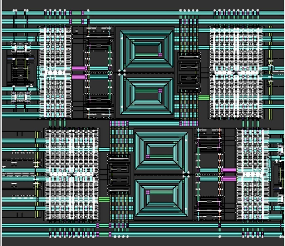
Samsung Foundry will use industry-leading electromagnetic (EM) simulation tools from Ansys (here for more information). This is to develop ultramodern projects, including 5G/6G, on the most advanced chips, nodes and process technologies. Ansys simulation solutions will provide a complete EM design flow. Ensuring greater capacity, speed and integration capability for Samsung’s most advanced semiconductor technology. And by accelerating on-chip design cycle times to increase high-speed connectivity while helping to reduce design errors and risks.
Samsung designers will leverage Ansys’ EM design tools. That is, Ansys RaptorX, Ansys VeloceRF e Ansys Exalt, to reduce time-to-market by two to three weeks for smaller projects and up to two months for complex projects. With automation capabilities that streamline computations and modeling, coupled with increased capacity, ANSYS ‘software will enable the Samsung team to design at faster speeds with greater fidelity.
Statements relating to new semiconductor projects by Samsung and Ansys
Below are the first statements on new semiconductor projects by Samsung and Ansys.
Electronic systems and process technologies are constantly evolving and therefore require state-of-the-art EM design capabilities,
he has declared Sangyun Kim, corporate vice president of Samsung Electronics’ Foundry Design Technology Team. Who then added:
We believe Ansys’ simulation solutions meet these challenges and will provide the highest level of expertise for our design needs. While reducing design time, cost and risk.
By integrating ANSYS EM solutions, Samsung designers can model complex on-chip scenarios, including dummy cards, which encompass millions of metal pieces in a fraction of the time. Additionally, Ansys’ near real-time modeling capabilities safeguard designs from electromagnetic interference. This helps significantly reduce the risk of chip failure.
EM is a primary challenge for chip designers as connectivity demands increase and technologies advance across the globe,
he has declared John Lee, vice president and general manager of the electronics, semiconductors and optics business unit of Ansys. Adding that:
At ANSYS, we make sure that our simulation solutions not only meet these growing demands, but remain state-of-the-art. We are confident that Ansys’ EM design portfolio is well equipped to provide the Samsung team with the tools they need to optimize their chip designs.
Ansys e Samsung have a long history of collaboration offering advanced solutions, including power integrity and electromigration approval solutions for low-power mobile and high-performance computing applications.
And you? what do you think of this new collaboration of Samsung and Ansys for the creation of new semiconductors ? tell us yours below in the comments and stay connected on TechGameWorld.com, for the latest news from the world of technology (and more!).
The article Samsung and Ansys: Together to Create New Semiconductor Projects comes from TechGameWorld.com.