
A new steo in the evolution of semiconductor technology: it is called VTFET transistor and was born from the collaboration of Samsung and IBM. This is a potential revolution because it promises drastic reductions in energy consumption
IBM and Samsung announce a new chip called VTFET, a turning point for semiconductors not only from the point of view of conventional design, but also and above all for potential in terms of performance and reduction of energy consumption – it is estimated that VTFET will require up to 85% less energy.
The VTFET transistor: a new technology for more efficient devices
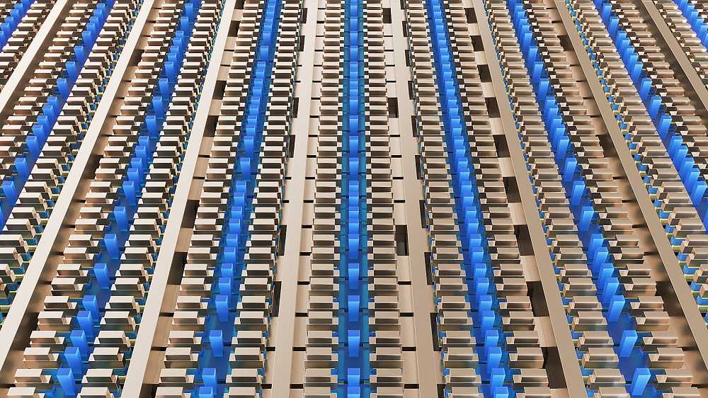
Developed by a joint team of researchers fromAlbany Nanotech Complex – one of the most advanced centers in semiconductor innovation globally – the revolutionary prototype from IBM and Samsung, new in design, has a vertical transistor architecture. This it allows an exponential number of transistors to be stacked vertically inside a chip, removing the density and energy efficiency constraints of current transistors, which are arranged horizontally to lie flat on the surface of a semiconductor.
https://www.youtube.com/watch?v=OF3Zwfu6Ngc
The resulting power reduction could lead to significant performance improvements in a variety of areas, such as:
- the cell phone batteries that can last more than a week without being charged, instead of days;
- energy-intensive processes, such as cryptomining operations and data encryption, which may require much less energy and have a lower impact on the carbon footprint;
- l’expansion of the Internet of Things (IoT) and edge devices that could be accelerated – requiring less energy to operate in harsh environments, such as ocean buoys, self-driving vehicles and spacecraft.
The Albany Nanotech Complex and IBM have also collaborated to produce the 2nm transistors, which allow to reach exceptional density with 50 billion transistors cram a space the size of a fingernail. The center is the result of billions of dollars in semiconductor R&D investments and is a shared public-private hub for scientific research and collaboration and is among the US government candidates for the National Semiconductor Technology Center. Dr. Mukesh Khare, Vice President, Hybrid Cloud and Systems, IBM Research, said:
This tech announcement is about defying conventions and rethinking how we continue to advance society and deliver new innovations that improve life, business and reduce our environmental footprint. Given the constraints the industry is currently facing on multiple fronts, IBM and Samsung are demonstrating our commitment to joint innovation in semiconductor design and a shared pursuit of what we call “hard tech”.
FinFET vs VTFET
The current technology most used in making chips is the FinFET one. Essentially the FinFET has the same structure as a traditional FET and therefore develops horizontally. This means that source, drain and gate lie roughly on the same plane. The term “Fin” derives from the fact that the suorce and drain channels are very thin and this allows to reach very high switching speeds and a higher density. However, a big problem remains: the consumption of area. Billions of transistors, however small, occupy a surface area. Increasing the number of transistors, keeping the compact size is more and more complicated in essence.
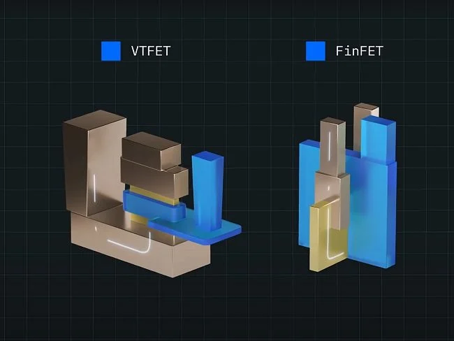
IBM and Samsun with VTFET transistor technology have succeeded instead create a transistor vertically. It means that the source is below, the gate is in the middle and the drain is above. A kind of sandwitch that would occupy much less area than a traditional transistor (a third theoretically). However, this structure would also improve the flow of current, thanks to a different design of the contact points between the components of the transist, allowing to save up to 85% of energy compared to FinFET technology.
The innovation at the Albany Nanotech Complex is geared towards commercialization and therefore it was announced that Samsung will produce the IBM chips with the 5nm node. These chips are expected to be used in IBM’s server platforms. The partnership dates back to 2018, when Samsung produced IBM’s 7nm chips, which became the foundation of the IBM Power10 server processor family earlier this year. The IBM Telum processor, also revealed earlier this year, is similarly manufactured by Samsung using IBM’s designs. IBM’s legacy of semiconductor innovations also includes the first implementation of 7nm and 5nm process technologies, high-k metal gate technology, SiGe channel transistors, single cell DRAM, Dennard scaling laws, amplified photoresists chemically, copper interconnect cabling, silicon over insulator technology, multi core microprocessors, embedded DRAM and 3D chip stacking.
Of course the real challenge for Samsung will be to succeed in produce these complicated three-dimensional structures efficiently and in high volumes. In fact, one of the enormous advantages of planar technology lies in the simplicity with which it is possible to produce chips. Sure it will be difficult to see VTFET transistor technology in commercial products soon, but it is still a huge achievement. That’s all from the hardware section, keep following us!